The Bionode
The Bionode originated between 2012 - 2013. All devices worked towards the same goal: creating the best device for bioelectric signal recording and stimulation in vivo utilizing wireless powering. This brief history will detail the key innovations that have taken place over the last 10 years.
Bionode History & Innovation
10+ Years of Innovation
The Bionode originated between 2012 - 2013 from a combination of the work done by Rebecca Bercich and Steven Lee in the Irazoqui Lab. The early devices up to the Bionode 3.2 were small enough to implant in mice. All devices worked towards the same goal: creating the best device for bioelectric signal recording and stimulation in vivo utilizing wireless powering. This brief history will detail the key innovations that have taken place over the last 10 years of Bionode development.
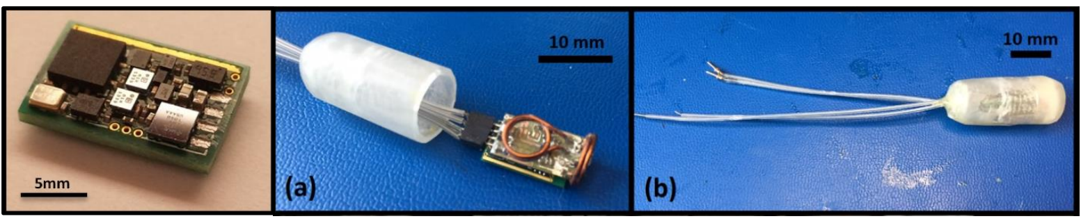
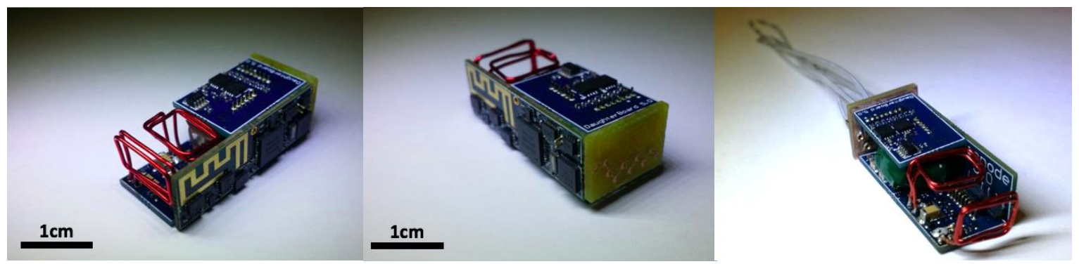
The first device, which was never fully standardized, was called the MioNode. It was small enough to implant in mice, recorded EMG signals (hence the name), and did not have a battery so it fully relied on wireless powering. The first standardized Bionode devices were the Bionode 2.0/2.1/2.2 in 2013 - 2014. There was a lot of innovation during this time so most of the details were not recorded. From a discovered Bionode 2 PCB, we found that this particular version has a chip antenna, nRF51822 BGA microcontroller, 2 recording channels similar to the topology used today, and stimulation capabilities. The stimulator had a 12-bit DAC, and there are a few rail-to-rail op amps and switches as well that most likely created a multiplexed stimulator as described for the Bionode 3.0. The board shown in Figure 1 was 20-by-6.5 mm including the removable programming header.
Bionode 3.0
The Bionode 3.0/3.2 were developed in 2014-2015. These devices were 2-board systems with a nRF51822 microcontroller, 2 AFE channels, a temperature sensor, 2 coils for wireless powering, and a straight printed communication antenna. The key features of these devices were the stimulators. The Bionode 3.0 used a DAC to set the voltage and then a switch to gate the output, creating square pulses. The two output electrodes were then multiplexed between the DAC output and ground to make one electrode appear positive and create a biphasic output. The Bionode 3.2 had a similar setup where a DAC set the voltage and a switch gated the output to create square pulses, but the output was amplified by a class AB output amplifier made of discrete transistors. With this, the electrodes did not have to be multiplexed as there was a true push-pull biphasic signal.
Bionode 4.0
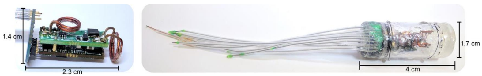
The Bionode 4.0/4.1, created during 2015 – 2016, was a 4-board system with a BGA nRF51822 microcontroller and 16 MHz crystal, 4 AFE channels split between 2 boards, a temperature sensor, a pressure sensor, 2 coils for wireless powering, and a straight printed communication antenna. A 340 MHz sine wave was used to charge a battery through two coils located on the power board. The device was typically packaged in a glass tube or 3D printed tube and implanted in a rat that lived in a 340 MHz resonant cavity. The stimulator utilized a 12-bit DAC7551, stim glitch switch, and Howland current pump (HCP) to create a biphasic current pulse that generates a push-pull biphasic stimulation. There was also a simple impedance measurement circuit to verifying the stimulation current and voltage, but it did not work very well. The stimulation function on the 4.0 board was discovered to be constantly stimulating the animal, so the stim glitch switch was added to the 4.1.
Bionode 5.0
The Bionode 5.0/5.1 (2018) was another 4-board system with a QFN nRF52832 microcontroller and 32 MHz crystal, 4 AFE channels on one board, 2 coils for wireless powering, and an inverted F printed communication antenna. This device had a working stimulator and a more sophisticated impedance measurement system so the Bionode Dataview UI could display the correct current and voltage pulse amplitudes. It was and still is the largest Bionode version. One of the issues with this device was that the wireless powering coupled onto the recording channels when the cavity was charging the battery. Due to the design of the device and the printed antenna, it could not be shielded from the RF signal.
The Bionode 5.2 (2019) went back to the 2-board system and that sought to fix the wireless powering problem and be implantable in a planar, flexible packaging. The mainboard houses 95% of the device’s components while the powernode is only needed for wireless powering. This device had the same components as the Bionode 5.1 except for a new digital-to-analog converter (DAC) and a quarter-wavelength whip antenna instead of a printed antenna. There is also only one coil for wireless powering which would be located at the spine of a rat when implanted. The wireless powering frequency was changed to 13.56 MHz because it is less likely to couple onto small traces unlike the 340MHz signal. This device worked well except the discontinued footprint was used for the power management IC (PMIC), making a redesign necessary. This board could be wrapped in copper tape to prevent any movement artifact during wireless powering.
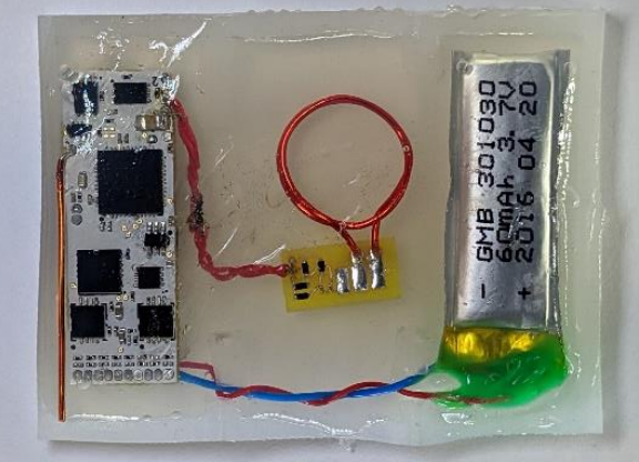
The Bionode 5.3 (2020) is a similar 2-board system to the 5.2, but the biggest change was the addition of 2 micro-SD style chips to facilitate the boards use in wearable use cases and the updated PMIC package. This device also allows access to 2 additional analog channels and 8 GPIO channels on the microcontroller. The battery voltage can be evaluated through Dataview. This design combined two separate level shifter components into one component and used smaller footprints for two other switches. Some of the current problems with this board is that there is not an isolated voltage source for the AFE (a problem that also would have occurring on the Bionode 5.2). Because of this, there is a stimulation artifact on the recording channels during stimulation. This can be fixed by adding an isolated 0.9V reference that only powers the AFE.
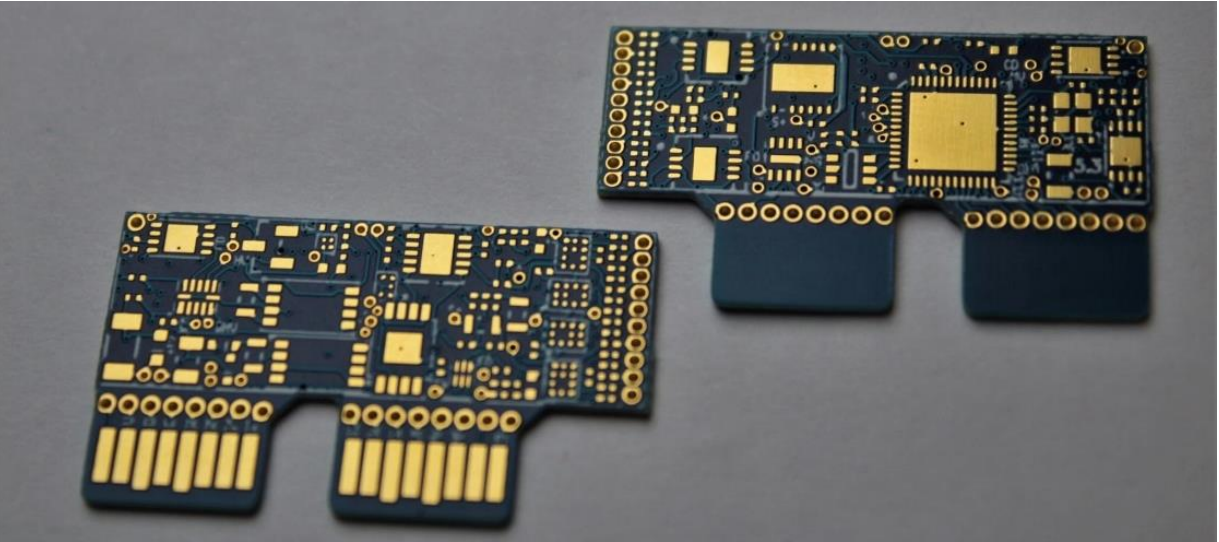
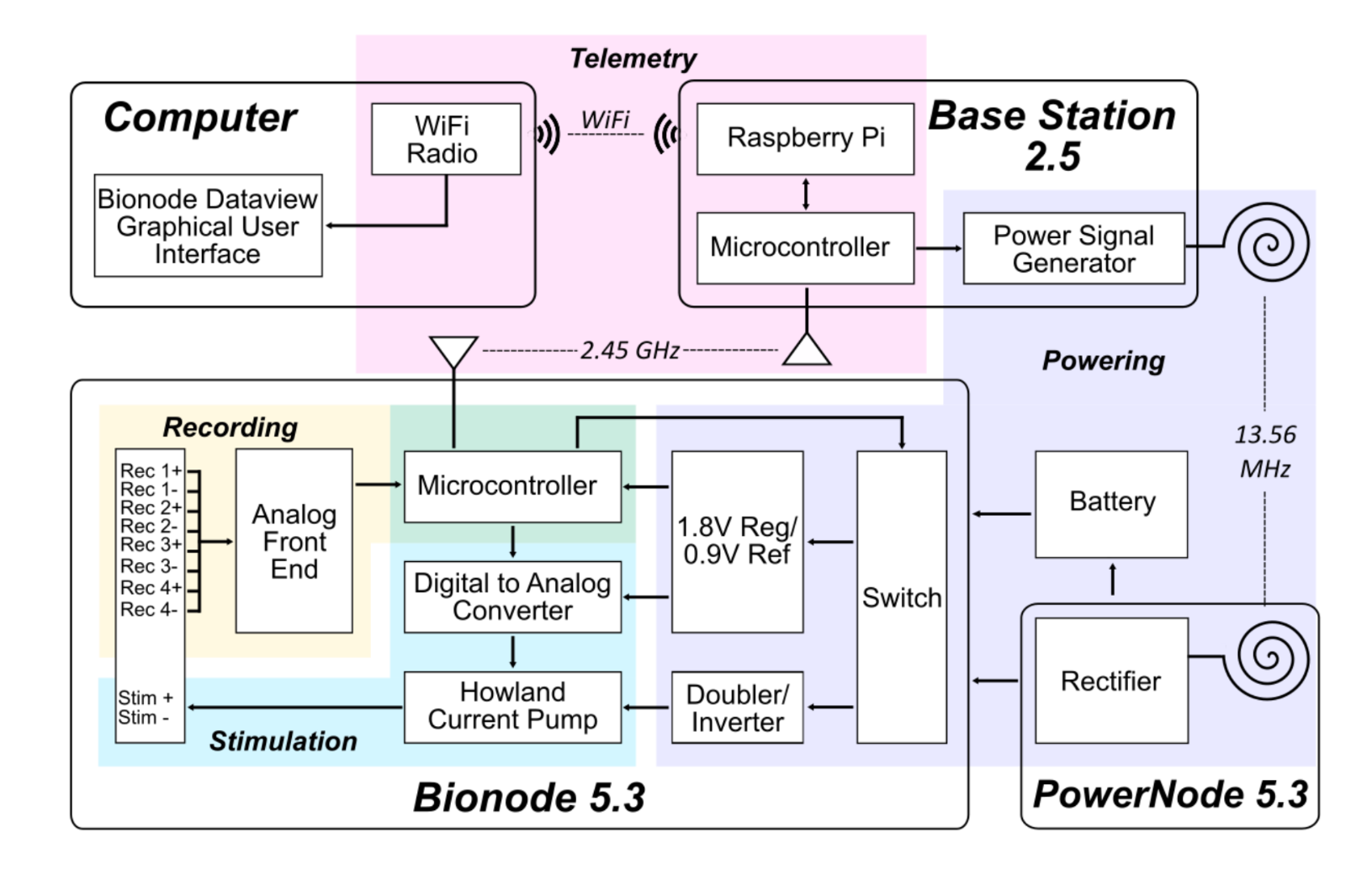
This Bionode, unlike its predecessors, only has one key board, denoted the Mainboard. This board houses the microcontroller, stimulator circuit, impedance measurement circuit, voltage sources and converters, battery charging circuitry, analog front end (AFE), and quarterwavelength whip communication antenna. The rectifying circuity, matching network, and powering coil are located on the Powernode. Through the Base Station, the user can give commands to the Bionode and receive recorded data from it. Figure 7 describes how all these units work together at a system level.
Bionode 6.0
To this day development continues with the Bionode 6.0.
Specifications
The Bionode 5.5 Characteristics
Features
- Wireless and battery powering,
- Wi-Fi/Radio communication,
- Nerve stimulation,
- Filtered signal recording
- Implantable
Power
- 3.7 V rails
- 1.8 V μC architecture
- 7 V stimulator, scalable to 12V for "pig" devices.
- Maximum Power Draw: 55.5 mW for rat, 81.4 mW for pig.
Stimulation Characteristics
- Parameters: Alternating Phase or Biphasic
- Pulse Amplitude: Max 3.7 V (adjustable on microamp scale with variable resistance)
- Pulse Width: adjustable on microsecond scale
- Stimulation Period: adjustable on microsecond scale
Recording parameters:
- Sample Frequencies: 500 Hz, 2.5 kHz, 5 kHz, and 12.5 kHz
- Up to 4 channels
- High Sample mode available
- ADC Resolution: 8, 10, or 12 bit
- Standard recordable signals: EKG, ECoG, CNAP, LFP, EGG, Respiration